用戶:Lijianqu/金剛石晶體缺陷
en:Crystallographic defects in diamond
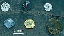
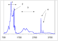
晶體結構的完美的周期性排列規律被破壞的情況稱為晶體缺陷,金剛石晶體缺陷是金剛石晶體中的常見現象。金剛石晶體缺陷產生的原因有多種,如晶格不規則性、外來替代雜質或填隙雜質,這些雜質可能是金剛石生長過程中或生長完成後引入的。晶體缺陷會影響金剛石材料性質,決定金剛石類型。金剛石最明顯受晶體缺陷影響的性質是顏色和電導率。晶體缺陷的影響可由能帶理論解釋。
金剛石晶體缺陷可由多種譜學技術檢測,如電子自旋共振(EPR)、 光致發光(PL)、電子束(陰極發光,CL)、紅外吸收光譜 (IR)、可見光和紫外光譜。吸收光譜學不僅用於識別缺陷,還能還能估算缺陷濃度,還能分辨天然鑽石與合成鑽石和優化鑽石。[1]
標定金剛石中心
[編輯]金剛石譜學裏有個傳統,用標有數字的字母縮寫標記缺陷致光譜,如GR1。這一傳統有值得注意的例外,如A、B、C中心。許多字母縮寫易使人混淆[2]:
- 有些符號太相似(如3H和H3)。
- 偶爾會有EPR和可見光譜用相同的符號標記不同的中心的情況,如N3 EPR中心與N3 可見光中心無任何關係[3]。
- 儘管很多字母縮寫是符合邏輯的,如N3(N是天然的(Natural)縮寫,用於天然鑽石),H3(H是加熱的(heated)縮寫,用於經加熱或輻照處理的鑽石), 許多縮寫沒有邏輯。特別是以下三個符合In particular, there is no clear distinction between the meaning of labels GR (普通輻射,general radiation), R (輻照,radiation) and TR (II型輻照,type-II radiation)沒有太大差別[2]。
缺陷對稱性
[編輯]晶體缺陷的對稱性用點群描述。晶體缺陷沒有空間平移對稱性,因此比晶體結構的對稱群要少。對於金剛石,目前為止,只發現具有如下對稱性的缺陷:四面體 (Td)、立方體l (D2d), 三方 (D3d、C3v)、菱形 (C2v)、單斜 (C2h、 C1h, C2) 和三斜 (C1 或 CS)[2][4]。
由缺陷對稱性可以預言很多光學性質。比如純金剛石不會有單光子(紅外)吸收,因為金剛石晶格具有反演中心。但是,如果有缺陷(即使是對稱性很高的缺陷,如N-N 置換對)破壞了晶體中心對稱性,就可以造成缺陷致紅外吸收,這是測量金剛石里缺陷濃度的最常見的方法[2]。
高溫高壓下的合成金剛石[5] 或化學氣相沉積方法合成金剛石[6][7],有對稱性低於四面體的缺陷在晶體生長方向排列。這種排列也見於砷化鎵[8],因此不是金剛石所獨有。
外來缺陷
[編輯]元素分析顯示,金剛石可含有多種雜質。金剛石里的雜質一般只有納米大小,在 光學顯微鏡下不可見。另外,任何元素都有可能通過離子注入進入金剛石。雜質元素進入金剛石更重要的途徑是在金剛石生長過程中以單個原子或小的原子團簇的形式進入金剛石晶體。到2008年,在金剛石中發現的雜質元素有氮、硼、氫、矽、 磷、 鎳、鈷,可能還有硫。已經確認金剛石中還會有錳[9] 和鎢[10],但是這兩種元素可能來自外來雜質。已檢測到金剛石中還有孤立的鐵原子[11],其來源後來有新的解釋,與金剛石合成過程中產生的紅寶石小粒子有關[12]。氧應該是金剛石中的主要雜質元素[13],但是還沒有光譜學證據 [來源請求]。發現有兩個電子自旋共振中心(OK1 and N3),認為來自氮氧複合物,但是只有間接證據支持,相應的濃度還非常低[14]。
氮
[編輯]金剛石中最常見的雜質是氮,在金剛石中的質量分數可達到1%[13]。以前人們認為,金剛石中所以的晶格缺陷都是結構異常造成的。後來研究發現,絕大多數金剛石都含有氮,並且構型多樣。含氮分子在進入金剛石前一般會分解,所以氮大多數情況下以單個原子的形式進入金剛石晶格,但是,金剛石晶體中也有氮分子存在[15]。
金剛石的光吸收和其他材料性質都與氮含量和聚集態密切相關。儘管所有的聚集構型都會導致紅外吸收,但是有些聚集形式常常是無色的,即幾乎不吸收任何 可見光[2]。四種主要的氮形式如下:
C-氮中心
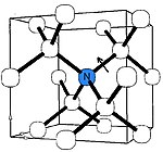
[編輯]C中心相應於電中性的單個取代氮原子,易見於These are easily seen in 電子順磁共振(EPR)譜[16](在EPR譜里又稱P1中心)。C中心使金剛石顏色呈深黃色到褐色,這樣的金剛石歸類為「Ib型」,俗稱「金絲雀鑽石」,為罕見的寶石類型。在高溫高壓下製備的合成金剛石絕大多數都含有高濃度的C-氮中心,其氮雜質來自大氣或石墨原料。每10萬碳原子有1個氮原子的金剛石帶有黃色[17]。因為氮原子有5個價電子,比被它取代的碳原子多一個,可以作為深電子施主,即每個取代氮原子可以多給出一個電子,在帶隙中形成一個施主能級。能量在約2.2 電子伏以上的光可以激發施主電子,使其進入 導帶,因而產生黃色[18]。
C中心的特徵紅外吸收光譜在1344 cm−1處有一個尖銳的峰,在1130 cm−1處有1個 較寬的特徵峰。在這些峰處的吸收一般用於測量單個氮原子雜質的濃度[19]。利用金剛石對波長約為260 nm的紫外光的吸收的測量方法因不可靠而被拋棄[18]。
金剛石中的受體缺陷會使C中心的氮原子成為離子,C中心轉化為C+中心。C+中心的特徵紅外吸收光譜在1332 cm−1處有1個明銳的峰,在1115, 、1046 and 和950 cm−1處有較寬較低的峰[20]。
A-氮中心
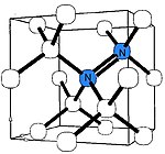
[編輯]A中心可能是天然金剛石最常見的缺陷。A中心中取代1個中性最近鄰氮原子對。A中心產生紫外吸收的閾值約為4 eV (310 nm, 即肉眼ke),因此不會使金剛石帶上顏色。含有以A中心的主的氮雜質歸類IaA型[21]。
A中心具有抗磁性,但是被紫外光或深受主離子化後會產生 電子順磁共振譜W24,分析此譜,確認氮N=N結構[22]。
The A center shows an IR absorption spectrum with no sharp features, which is distinctly different from that of the C or B centers. Its strongest peak at 1282 cm−1 is routinely used to estimate the nitrogen concentration in the A form.[23]
B-nitrogen center
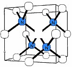
[編輯]There is a general consensus that B center (sometimes called B1) consists of a carbon vacancy surrounded by four nitrogen atoms substituting for carbon atoms.[1][2][24] This model is consistent with other experimental results, but there is no direct spectroscopic data corroborating it. Diamonds where most nitrogen forms B centers are rare and are classed as type IaB; most gem diamonds contain a mixture of A and B centers, together with N3 centers.
Similar to the A centers, B centers do not induce color, and no UV or visible absorption can be attributed to the B centers. Early assignment of the N9 absorption system to the B center have been disproven later.[25] The B center has a characteristic IR absorption spectrum (see the infrared absorption picture above) with a sharp peak at 1332 cm−1 and a broader feature at 1280 cm−1. The latter is routinely used to estimate the nitrogen concentration in the B form.[26]
Note that many optical peaks in diamond accidentally have similar spectral positions, which causes much confusion among gemologists. Spectroscopists use for defect identification the whole spectrum rather than one peak, and consider the history of the growth and processing of individual diamond.[1][2][24]
N3 nitrogen center
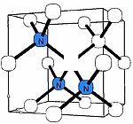
[編輯]The N3 center consists of three nitrogen atoms surrounding a vacancy. Its concentration is always just a fraction of the A and B centers.[27] The N3 center is paramagnetic, so its structure is well justified from the analysis of the EPR spectrum P2.[3] This defect produces a characteristic absorption and luminescence line at 415 nm and thus does not induce color on its own. However, the N3 center is always accompanied by the N2 center, having an absorption line at 478 nm (and no luminescence).[28] As a result, diamonds rich in N3/N2 centers are yellow in color.
Boron
[編輯]Diamonds containing boron as a substitutional impurity are termed type IIb. Only one percent of natural diamonds are of this type, and most are blue to grey.[29] Boron is an acceptor in diamond: boron atoms have one less available electron than the carbon atoms; therefore, each boron atom substituting for a carbon atom creates an electron hole in the band gap that can accept an electron from the valence band. This allows red light absorption, and due to the small energy (0.37 eV)[30] needed for the electron to leave the valence band, holes can be thermally released from the boron atoms to the valence band even at room temperatures. These holes can move in an electric field and render the diamond electrically conductive (i.e., a p-type semiconductor). Very few boron atoms are required for this to happen—a typical ratio is one boron atom per 1,000,000 carbon atoms.
Boron-doped diamonds transmit light down to ~250 nm and absorb some red and infrared light (hence the blue color); they may phosphoresce blue after exposure to shortwave ultraviolet light.[30] Apart from optical absorption, boron acceptors have been detected by electron paramagnetic resonance.[31]
Phosphorus
[編輯]Phosphorus could be intentionally introduced into diamond grown by chemical vapor deposition (CVD) at concentrations up to ~0.01%.[32] Phosphorus substitutes carbon in the diamond lattice.[33] Similar to nitrogen, phosphorus has one more electron than carbon and thus acts as a donor; however, the ionization energy of phosphorus (0.6 eV)[32] is much smaller than that of nitrogen (1.7 eV)[34] and is small enough for room-temperature thermal ionization. This important property of phosphorus in diamond favors electronic applications, such as UV light emitting diodes (LEDs, at 235 nm).[35]
Hydrogen
[編輯]Hydrogen is one of the most technological important impurities in semiconductors, including diamond. Hydrogen-related defects are very different in natural diamond and in synthetic diamond films. Those films are produced by various chemical vapor deposition (CVD) techniques in an atmosphere rich in hydrogen (typical hydrogen/carbon ratio >100), under strong bombardment of growing diamond by the plasma ions. As a result, CVD diamond is always rich in hydrogen and lattice vacancies. In polycrystalline films, much of the hydrogen may be located at the boundaries between diamond 'grains', or in non-diamond carbon inclusions. Within the diamond lattice itself, hydrogen-vacancy[36] and hydrogen-nitrogen-vacancy[37] complexes have been identified in negative charge states by electron paramagnetic resonance. In addition, numerous hydrogen-related IR absorption peaks are documented.[38]
It is experimentally demonstrated that hydrogen passivates electrically active boron[39] and phosphorus[40] impurities. As a result of such passivation, shallow donor centers are presumably produced.[41]
In natural diamonds, several hydrogen-related IR absorption peaks are commonly observed; the strongest ones are located at 1405, 3107 and 3237 cm−1 (see IR absorption figure above). The microscopic structure of the corresponding defects is yet unknown and it is not even certain whether or not those defects originate in diamond or in foreign inclusions. Gray color in some diamonds from the Argyle mine in Australia is often associated with those hydrogen defects, but again, this assignment is yet unproven.[42]
Nickel and cobalt
[編輯]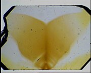

When diamonds are grown by the high-pressure high-temperature technique, nickel, cobalt or some other metals are usually added into the growth medium to facilitate catalytically the conversion of graphite into diamond. As a result, metallic inclusions are formed. Besides, isolated nickel and cobalt atoms incorporate into diamond lattice, as demonstrated through characteristic hyperfine structure in electron paramagnetic resonance, optical absorption and photoluminescence spectra,[43] and the concentration of isolated nickel can reach 0.01%.[44] This fact is by all means unusual considering the large difference in size between carbon and transition metal atoms and the superior rigidity of the diamond lattice.[2][44]
Numerous Ni-related defects have been detected by electron paramagnetic resonance,[5][45] optical absorption and photoluminescence,[5][45][46] both in synthetic and natural diamonds.[42] Three major structures can be distinguished: substitutional Ni,[47] nickel-vacancy[48] and nickel-vacancy complex decorated by one or more substitutional nitrogen atoms.[45] The "nickel-vacancy" structure, also called "semi-divacancy" is specific for most large impurities in diamond and silicon (e.g., tin in silicon[49]). Its production mechanism is generally accepted as follows: large nickel atom incorporates substitutionally, then expels a nearby carbon (creating a neighboring vacancy), and shifts in-between the two sites.
Although the physical and chemical properties of cobalt and nickel are rather similar, the concentrations of isolated cobalt in diamond are much smaller than those of nickel (parts per billion range). Several defects related to isolated cobalt have been detected by electron paramagnetic resonance[50] and photoluminescence,[5][51] but their structure is yet unknown.[52]
Silicon
[編輯]
Silicon is a common impurity in diamond films grown by chemical vapor deposition and it originates either from silicon substrate or from silica windows or walls of the CVD reactor. It was also observed in natural diamonds in dispersed form.[53] Isolated silicon defects have been detected in diamond lattice through the sharp optical absorption peak at 738 nm[54] and electron paramagnetic resonance.[55] Similar to other large impurities, the major form of silicon in diamond has been identified with a Si-vacancy complex (semi-divacancy site).[55] This center is a deep donor having an ionization energy of 2 eV, and thus again is unsuitable for electronic applications.[56]
Si-vacancies constitute minor fraction of total silicon. It is believed (though no proof exists) that much silicon substitutes for carbon thus becoming invisible to most spectroscopic techniques because silicon and carbon atoms have the same configuration of the outer electronic shells.[57]
Sulfur
[編輯]Around the year 2000, there was a wave of attempts to dope synthetic CVD diamond films by sulfur aiming at n-type conductivity with low activation energy. Successful reports have been published,[58] but then dismissed[59] as the conductivity was rendered p-type instead of n-type and associated not with sulfur, but with residual boron, which is a highly efficient p-type dopant in diamond.
So far (2009), there is only one reliable evidence (through hyperfine interaction structure in electron paramagnetic resonance) for isolated sulfur defects in diamond. The corresponding center called W31 has been observed in natural type-Ib diamonds in small concentrations (parts per million). It was assigned to a sulfur-vacancy complex – again, as in case of nickel and silicon, a semi-divacancy site.[60]
參見
[編輯]參考資料
[編輯]- ^ 1.0 1.1 1.2 Alan T. Collins. The detection of colour-enhanced and synthetic gem diamonds by optical spectroscopy. Diamond and Related Materials. 2003-10, 12 (10-11): 1976–1983 [2019-06-25]. doi:10.1016/S0925-9635(03)00262-0 (英語).
- ^ 2.0 2.1 2.2 2.3 2.4 2.5 2.6 2.7 J Walker. Optical absorption and luminescence in diamond. Reports on Progress in Physics. 1979-10-01, 42 (10): 1605–1659 [2019-06-25]. ISSN 0034-4885. doi:10.1088/0034-4885/42/10/001.
- ^ 3.0 3.1 J A van Wyk. Carbon-12 hyperfine interaction of the unique carbon of the P2 (ESR) or N3 (optical) centre in diamond. Journal of Physics C: Solid State Physics. 1982-09-30, 15 (27): L981–L983 [2019-06-25]. ISSN 0022-3719. doi:10.1088/0022-3719/15/27/007.
- ^ Zaitsev, A. M. Optical Properties of Diamond : A Data Handbook. Springer. 2001. ISBN 3-540-66582-X.
- ^ 5.0 5.1 5.2 5.3 K Iakoubovskii, A T Collins. Alignment of Ni- and Co-related centres during the growth of high-pressure–high-temperature diamond. Journal of Physics: Condensed Matter. 2004-10-06, 16 (39): 6897–6906 [2019-06-25]. ISSN 0953-8984. doi:10.1088/0953-8984/16/39/022.
- ^ A. M. Edmonds, U. F. S. D』Haenens-Johansson, R. J. Cruddace, M. E. Newton, K.-M. C. Fu, C. Santori, R. G. Beausoleil, D. J. Twitchen, M. L. Markham. Production of oriented nitrogen-vacancy color centers in synthetic diamond. Physical Review B. 2012-07-05, 86 (3) [2019-06-25]. ISSN 1098-0121. doi:10.1103/PhysRevB.86.035201 (英語).
- ^ U. F. S. D』Haenens-Johansson, A. M. Edmonds, M. E. Newton, J. P. Goss, P. R. Briddon, J. M. Baker, P. M. Martineau, R. U. A. Khan, D. J. Twitchen, S. D. Williams. EPR of a defect in CVD diamond involving both silicon and hydrogen that shows preferential alignment. Physical Review B. 2010-10-15, 82 (15) [2019-06-25]. ISSN 1098-0121. doi:10.1103/PhysRevB.82.155205 (英語).
- ^ R. A. Hogg, K. Takahei, A. Taguchi, Y. Horikoshi. Preferential alignment of Er–2O centers in GaAs:Er,O revealed by anisotropic host‐excited photoluminescence. Applied Physics Letters. 1996-06-03, 68 (23): 3317–3319 [2019-06-25]. ISSN 0003-6951. doi:10.1063/1.116043 (英語).
- ^ K. Iakoubovskii, A. Stesmans. Characterization of Defects in as-Grown CVD Diamond Films and HPHT Diamond Powders by Electron Paramagnetic Resonance. physica status solidi (a). 2001-08, 186 (2): 199–206 [2020-07-07]. ISSN 0031-8965. doi:10.1002/1521-396X(200108)186:23.0.CO;2-R (英語).
- ^ S. Lal, T. Dallas, S. Yi, S. Gangopadhyay, M. Holtz, F. G. Anderson. Defect photoluminescence in polycrystalline diamond films grown by arc-jet chemical-vapor deposition. Physical Review B. 1996-11-15, 54 (19): 13428–13431 [2019-06-25]. ISSN 0163-1829. doi:10.1103/PhysRevB.54.13428 (英語).
- ^ K Iakoubovskii, G J Adriaenssens. Evidence for a Fe-related defect centre in diamond. Journal of Physics: Condensed Matter. 2002-02-04, 14 (4): L95–L98 [2019-06-25]. ISSN 0953-8984. doi:10.1088/0953-8984/14/4/104.
- ^ Konstantin Iakoubovskii, Guy J Adriaenssens. Comment on `Evidence for a Fe-related defect centre in diamond'. Journal of Physics: Condensed Matter. 2002-06-03, 14 (21): 5459–5460 [2019-06-25]. doi:10.1088/0953-8984/14/21/401.
- ^ 13.0 13.1 W. Kaiser, W. L. Bond. Nitrogen, A Major Impurity in Common Type I Diamond. Physical Review. 1959-08-15, 115 (4): 857–863 [2019-06-25]. ISSN 0031-899X. doi:10.1103/PhysRev.115.857 (英語).
- ^ M E Newton, J M Baker. 14 N ENDOR of the OK1 centre in natural type Ib diamond. Journal of Physics: Condensed Matter. 1989-12-25, 1 (51): 10549–10561 [2019-06-25]. ISSN 0953-8984. doi:10.1088/0953-8984/1/51/024.
- ^ Konstantin Iakoubovskii, Guy J Adriaenssens, Yogesh K Vohra. Nitrogen incorporation in diamond films homoepitaxially grown by chemical vapour deposition. Journal of Physics: Condensed Matter. 2000-07-31, 12 (30): L519–L524 [2019-06-25]. ISSN 0953-8984. doi:10.1088/0953-8984/12/30/106.
- ^ W. V. Smith, P. P. Sorokin, I. L. Gelles, G. J. Lasher. Electron-Spin Resonance of Nitrogen Donors in Diamond. Physical Review. 1959-09-15, 115 (6): 1546–1552 [2019-06-25]. ISSN 0031-899X. doi:10.1103/PhysRev.115.1546 (英語).
- ^ Nassau, Kurt (1980) "Gems made by man" Gemological Institute of America, Santa Monica, California, ISBN 0-87311-016-1, p. 191
- ^ 18.0 18.1 K Iakoubovskii, G J Adriaenssens. Optical transitions at the substitutional nitrogen centre in diamond. Journal of Physics: Condensed Matter. 2000-02-14, 12 (6): L77–L81 [2019-06-25]. ISSN 0953-8984. doi:10.1088/0953-8984/12/6/102.
- ^ I. Kiflawi et al. "Infrared-absorption by the single nitrogen and a defect centers in diamond" Phil. Mag. B 69 (1994) 1141
- ^ Simon C Lawson, David Fisher, Damian C Hunt, Mark E Newton. On the existence of positively charged single-substitutional nitrogen in diamond. Journal of Physics: Condensed Matter. 1998-07-13, 10 (27): 6171–6180 [2019-06-25]. ISSN 0953-8984. doi:10.1088/0953-8984/10/27/016.
- ^ G Davies. The A nitrogen aggregate in diamond-its symmetry and possible structure. Journal of Physics C: Solid State Physics. 1976-10-14, 9 (19): L537–L542 [2019-06-25]. ISSN 0022-3719. doi:10.1088/0022-3719/9/19/005.
- ^ O. D. Tucker, M. E. Newton, J. M. Baker. EPR and N 14 electron-nuclear double-resonance measurements on the ionized nearest-neighbor dinitrogen center in diamond. Physical Review B. 1994-12-01, 50 (21): 15586–15596 [2019-06-25]. ISSN 0163-1829. doi:10.1103/PhysRevB.50.15586 (英語).
- ^ S. R. Boyd, I. Kiflawi, G. S. Woods. The relationship between infrared absorption and the A defect concentration in diamond. Philosophical Magazine B. 1994-06, 69 (6): 1149–1153 [2019-06-25]. ISSN 1364-2812. doi:10.1080/01418639408240185 (英語).
- ^ 24.0 24.1 引用錯誤:沒有為名為
collins2的參考文獻提供內容 - ^ A.A. Shiryaev, M.T. Hutchison, K.A. Dembo, A.T. Dembo, K. Iakoubovskii, Yu.A. Klyuev, A.M. Naletov. High-temperature high-pressure annealing of diamond. Physica B: Condensed Matter. 2001-12,. 308-310: 598–603 [2019-06-25]. doi:10.1016/S0921-4526(01)00750-5 (英語).
- ^ S. R. Boyd, I. Kiflawi, G. S. Woods. Infrared absorption by the B nitrogen aggregate in diamond. Philosophical Magazine B. 1995-09, 72 (3): 351–361 [2019-06-25]. ISSN 1364-2812. doi:10.1080/13642819508239089 (英語).
- ^ Anderson, B.; Payne, J.; Mitchell, R.K. (ed.) (1998) "The spectroscope and gemology", p. 215, Robert Hale Limited, Clerkwood House, London. ISBN 0-7198-0261-X
- ^ M. F. Thomaz, G. Davies. The Decay Time of N3 Luminescence in Natural Diamond. Proceedings of the Royal Society A: Mathematical, Physical and Engineering Sciences. 1978-08-22, 362 (1710): 405–419 [2019-06-25]. ISSN 1364-5021. doi:10.1098/rspa.1978.0141 (英語).
- ^ O'Donoghue, M. (2002) "Synthetic, imitation & treated gemstones", Elsevier Butterworth-Heinemann, Great Britain. ISBN 0-7506-3173-2, p. 52
- ^ 30.0 30.1 The optical and electronic properties of semiconducting diamond. Philosophical Transactions of the Royal Society of London. Series A: Physical and Engineering Sciences. 1993-02-15, 342 (1664): 233–244 [2019-06-25]. ISSN 0962-8428. doi:10.1098/rsta.1993.0017 (英語).
- ^ C A J Ammerlaan, R van Kemp. Magnetic resonance spectroscopy in semiconducting diamond. Journal of Physics C: Solid State Physics. 1985-05-10, 18 (13): 2623–2629 [2019-06-25]. ISSN 0022-3719. doi:10.1088/0022-3719/18/13/009.
- ^ 32.0 32.1 T. Kociniewski, J. Barjon, M.-A. Pinault, F. Jomard, A. Lusson, D. Ballutaud, O. Gorochov, J. M. Laroche, E. Rzepka, J. Chevallier, C. Saguy. n-type CVD diamond doped with phosphorus using the MOCVD technology for dopant incorporation. physica status solidi (a). 2006-09, 203 (12): 3136–3141 [2019-06-25]. doi:10.1002/pssa.200671113 (英語).
- ^ Masataka Hasegawa, Tokuyuki Teraji, Satoshi Koizumi. Lattice location of phosphorus in n -type homoepitaxial diamond films grown by chemical-vapor deposition. Applied Physics Letters. 2001-11-05, 79 (19): 3068–3070 [2019-06-25]. ISSN 0003-6951. doi:10.1063/1.1417514 (英語).
- ^ R.G. Farrer. On the substitutional nitrogen donor in diamond. Solid State Communications. 1969-05, 7 (9): 685–688 [2019-06-25]. doi:10.1016/0038-1098(69)90593-6 (英語).
- ^ S. Koizumi. Ultraviolet Emission from a Diamond pn Junction. Science. 2001-06-08, 292 (5523): 1899–1901 [2019-06-25]. doi:10.1126/science.1060258.
- ^ Claire Glover, M. E. Newton, P. M. Martineau, Samantha Quinn, D. J. Twitchen. Hydrogen incorporation in diamond: the vacancy-hydrogen complex. Physical Review Letters. 2004-04-02, 92 (13): 135502 [2019-06-25]. ISSN 0031-9007. PMID 15089622. doi:10.1103/PhysRevLett.92.135502.
- ^ Claire Glover, M. E. Newton, P. Martineau, D. J. Twitchen, J. M. Baker. Hydrogen Incorporation in Diamond: The Nitrogen-Vacancy-Hydrogen Complex. Physical Review Letters. 2003-05-09, 90 (18) [2019-06-25]. ISSN 0031-9007. doi:10.1103/PhysRevLett.90.185507 (英語).
- ^ F. Fuchs, C. Wild, K. Schwarz, W. Müller‐Sebert, P. Koidl. Hydrogen induced vibrational and electronic transitions in chemical vapor deposited diamond, identified by isotopic substitution. Applied Physics Letters. 1995-01-09, 66 (2): 177–179 [2019-06-25]. ISSN 0003-6951. doi:10.1063/1.113126 (英語).
- ^ J. Chevallier, B. Theys, A. Lusson, C. Grattepain, A. Deneuville, E. Gheeraert. Hydrogen-boron interactions in p -type diamond. Physical Review B. 1998-09-15, 58 (12): 7966–7969 [2019-06-25]. ISSN 0163-1829. doi:10.1103/PhysRevB.58.7966 (英語).
- ^ J Chevallier, F Jomard, Z Teukam, S Koizumi, H Kanda, Y Sato, A Deneuville, M Bernard. Hydrogen in n-type diamond. Diamond and Related Materials. 2002-08, 11 (8): 1566–1571 [2019-06-25]. doi:10.1016/S0925-9635(02)00063-8 (英語).
- ^ Zéphirin Teukam, Jacques Chevallier, Cécile Saguy, Rafi Kalish, Dominique Ballutaud, Michel Barbé, François Jomard, Annie Tromson-Carli, Catherine Cytermann, James E. Butler, Mathieu Bernard, Céline Baron, Alain Deneuville. Shallow donors with high n-type electrical conductivity in homoepitaxial deuterated boron-doped diamond layers. Nature Materials. 2003-07, 2 (7): 482–486 [2019-06-25]. ISSN 1476-1122. doi:10.1038/nmat929 (英語).
- ^ 42.0 42.1 K Iakoubovskii, G.J Adriaenssens. Optical characterization of natural Argyle diamonds. Diamond and Related Materials. 2002-01, 11 (1): 125–131 [2019-06-25]. doi:10.1016/S0925-9635(01)00533-7 (英語).
- ^ Konstantin Iakoubovskii, Gordon Davies. Vibronic effects in the 1.4 − eV optical center in diamond. Physical Review B. 2004-12-09, 70 (24) [2019-06-25]. ISSN 1098-0121. doi:10.1103/PhysRevB.70.245206 (英語).
- ^ 44.0 44.1 Alan T. Collins, Hisao Kanda, J. Isoya, C.A.J. Ammerlaan, J.A. van Wyk. Correlation between optical absorption and EPR in high-pressure diamond grown from a nickel solvent catalyst. Diamond and Related Materials. 1998-02, 7 (2-5): 333–338 [2019-06-25]. doi:10.1016/S0925-9635(97)00270-7 (英語).
- ^ 45.0 45.1 45.2 V A Nadolinny, A P Yelisseyev, J M Baker, M E Newton, D J Twitchen, S C Lawson, O P Yuryeva, B N Feigelson. A study of 13 C hyperfine structure in the EPR of nickel-nitrogen-containing centres in diamond and correlation with their optical properties. Journal of Physics: Condensed Matter. 1999-09-27, 11 (38): 7357–7376 [2019-06-25]. ISSN 0953-8984. doi:10.1088/0953-8984/11/38/314.
- ^ Larico, R.; Justo, J. F.; Machado, W. V. M.; Assali, L. V. C. Electronic properties and hyperfine fields of nickel-related complexes in diamond. Phys. Rev. B. 2009, 79: 115202. doi:10.1103/PhysRevB.79.115202.
- ^ J. Isoya, H. Kanda, J. R. Norris, J. Tang, M. K. Bowman. Fourier-transform and continuous-wave EPR studies of nickel in synthetic diamond: Site and spin multiplicity. Physical Review B. 1990-03-01, 41 (7): 3905–3913 [2019-06-25]. ISSN 0163-1829. doi:10.1103/PhysRevB.41.3905 (英語).
- ^ K. Iakoubovskii. Ni-vacancy defect in diamond detected by electron spin resonance. Physical Review B. 2004-11-19, 70 (20) [2019-06-25]. ISSN 1098-0121. doi:10.1103/PhysRevB.70.205211 (英語).
- ^ G. D. Watkins. Defects in irradiated silicon: EPR of the tin-vacancy pair. Physical Review B. 1975-11-15, 12 (10): 4383–4390 [2019-06-25]. ISSN 0556-2805. doi:10.1103/PhysRevB.12.4383 (英語).
- ^ D. J. Twitchen, J. M. Baker, M. E. Newton, K. Johnston. Identification of cobalt on a lattice site in diamond. Physical Review B. 2000-01-01, 61 (1): 9–11 [2019-06-25]. ISSN 0163-1829. doi:10.1103/PhysRevB.61.9 (英語).
- ^ Simon C. Lawson, Hisao Kanda, Kenji Watanabe, Isaac Kiflawi, Yoichiro Sato, Alan T. Collins. Spectroscopic study of cobalt-related optical centers in synthetic diamond. Journal of Applied Physics. 1996, 79 (8): 4348 [2019-06-25]. doi:10.1063/1.361744 (英語).
- ^ Larico, R.; Assali, L. V. C.; Machado, W. V. M.; Justo, J. F. Cobalt-related impurity centers in diamond: electronic properties and hyperfine parameters. J. Phys.: Condens. Matter. 2008, 20: 415220. doi:10.1088/0953-8984/20/41/415220.
- ^ K. Iakoubovskii, G.J. Adriaenssens, N.N. Dogadkin, A.A. Shiryaev. Optical characterization of some irradiation-induced centers in diamond. Diamond and Related Materials. 2001-01, 10 (1): 18–26 [2019-06-25]. doi:10.1016/S0925-9635(00)00361-7 (英語).
- ^ C. D. Clark, H. Kanda, I. Kiflawi, G. Sittas. Silicon defects in diamond. Physical Review B. 1995-06-15, 51 (23): 16681–16688 [2019-06-25]. ISSN 0163-1829. doi:10.1103/PhysRevB.51.16681 (英語).
- ^ 55.0 55.1 A. M. Edmonds, M. E. Newton, P. M. Martineau, D. J. Twitchen, S. D. Williams. Electron paramagnetic resonance studies of silicon-related defects in diamond. Physical Review B. 2008-06-11, 77 (24) [2019-06-25]. ISSN 1098-0121. doi:10.1103/PhysRevB.77.245205 (英語).
- ^ K. Iakoubovskii, G. J. Adriaenssens. Luminescence excitation spectra in diamond. Physical Review B. 2000-04-15, 61 (15): 10174–10182 [2019-06-25]. ISSN 0163-1829. doi:10.1103/PhysRevB.61.10174 (英語).
- ^ U. F. S. D'Haenens-Johansson, A. M. Edmonds, B. L. Green, M. E. Newton, G. Davies, P. M. Martineau, R. U. A. Khan, D. J. Twitchen. Optical properties of the neutral silicon split-vacancy center in diamond. Physical Review B. 2011-12-21, 84 (24) [2019-06-25]. ISSN 1098-0121. doi:10.1103/PhysRevB.84.245208 (英語).
- ^ Isao Sakaguchi, Mikka N.-Gamo, Yuko Kikuchi, Eiji Yasu, Hajime Haneda, Toshimitsu Suzuki, Toshihiro Ando. Sulfur: A donor dopant for n -type diamond semiconductors. Physical Review B. 1999-07-15, 60 (4): R2139–R2141 [2019-06-25]. ISSN 0163-1829. doi:10.1103/PhysRevB.60.R2139 (英語).
- ^ R. Kalish, A. Reznik, C. Uzan-Saguy, C. Cytermann. Is sulfur a donor in diamond?. Applied Physics Letters. 2000-02-07, 76 (6): 757–759 [2019-06-25]. ISSN 0003-6951. doi:10.1063/1.125885 (英語).
- ^ J. M. Baker, J. A. van Wyk, J. P. Goss, P. R. Briddon. Electron paramagnetic resonance of sulfur at a split-vacancy site in diamond. Physical Review B. 2008-12-12, 78 (23) [2019-06-25]. ISSN 1098-0121. doi:10.1103/PhysRevB.78.235203 (英語).
